
SEM, EDS
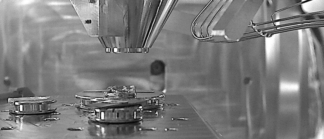
SEM (Scanning Electron Microscopy): Thermo Scientific Apreo
This SEM can be used for high-resolution imaging and to obtain compositional and elemental information of the surface or near-surface region of different samples.
SEM is useful for materials science and for industrial manufacturing and can be used to image materials ranging e.g. from nano- and microparticles, catalysts, and nanodevices to bulk magnetic samples and insulators such as polymers. This SEM has broad analytical extensions: STEM (Scanning Transmission Electron Microscopy), CLD (Cathodoluminescence detector) and EDS (Energy-dispersive X-ray detector).
For more information, contact Ermei Mäkilä.