Semiconductors and Memory

Boosting the Efficiency of Semiconductor Devices with Atomistic Interface Control
Project Lead: Konstantinos Konstantinou
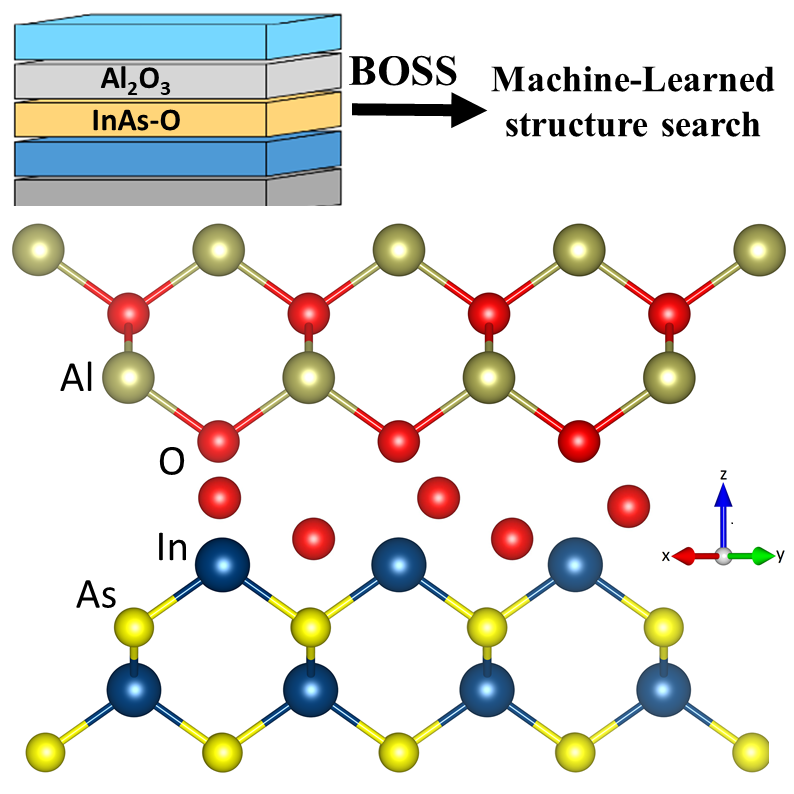
This is a Tandem Industry-Academia project funded by the Finnish Research Impact Foundation. The aim is to determine the atomic-scale geometry and the electronic structure at the interface formation between InAs(100)-O and Al2O3 surfaces with a Bayesian Optimization Structure Search (BOSS) approach and Density Functional Theory (DFT) calculations. The acquired knowledge will be applied in multi-scale simulations of the entire semiconductor device, to generate predictive models for products of interest relevant to the industrial collaborator.
Partner(s): Comptek Solutions Oy, Turku

AI-driven computational study of ALD growth on semiconductor wafers
Project Lead: Elli Virtanen
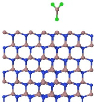
Atomic layer deposition is important for growing defect-free, high-performance semiconductor wafers for next-generation technologies. We deploy atomistic structure search to explore which ALD precursor molecules are best suited for facilitating the growth of GaN thin films.

Unlocking non-equilibrium processes in resistive switching memory and selector devices (NoneqRSMSD)
Project Lead: Konstantinos Konstantinou
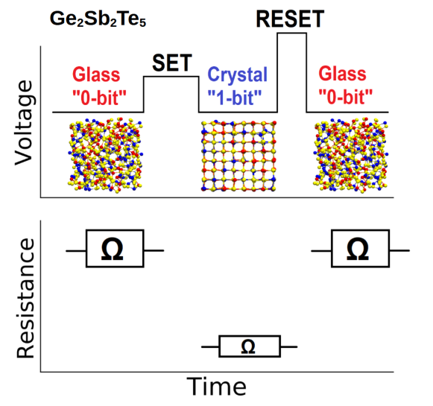
Energy efficiency of future computing is achievable through the transition from processor-centric to memory-centric architectures. This project aims to achieve a thorough knowledge and a comprehensive understanding of ion-irradiation processes in chalcogenide phase-change memory materials with atomistic simulations. Computational experiments will be performed to tackle key fundamental challenges and technological issues, to obtain improved functional memory devices for next-generation computer hardware.
Partner(s): Prof Stephen Elliott, University of Oxford, UK, Prof Emilio Artacho, CIC-Nanogune, Spain, Dr Miguel Caro, Aalto University, Finland
